
Annotated rendering of the front of the card
Curious how the holiday card does the things it does? Well, here you read all of the gritty technical details.
At its core, the card harvests energy from light, radio, and/or a USB connection to enable the blinking of LEDs. If there's an excess of energy available, it will store some of that excess in a supercapacitor so that it's able to run for a while when no other sources of energy are available.
So far, so good, and so ordinary (especially when connected via USB). The magic of the system, and the cause of its complexity, is in its efficiency. For example, the system can run on as little as 200 lux of light (albeit intermittently), but how can it do so with no solar cells? For another example, the card can run on latent 2.4 GHz radio energy, such as from your WiFi network, but how can there be enough power there to do anything useful?
The tricks go beyond just harvesting power. The card can receive commands from any modern phone via any 2.4 GHz WiFi network -- yes, any network, even if it's secured with the best encryption and without the card having the network password. How? We'll explore that later on this page.
The hardware can be separated into three high-level groups: energy accumulation, energy consumption, and energy control.
Hardware focused on energy accumulation includes the light-harvesting LEDS, the 2.4 GHz radio, the USB-C port, and sometimes the supercapacitor.
The decorative LEDs are the primary consumers of energy.
Finally, hardware that is mostly for the control of energy is the microcontroller and the rail interconnect.

Annotated rendering of the front of the card
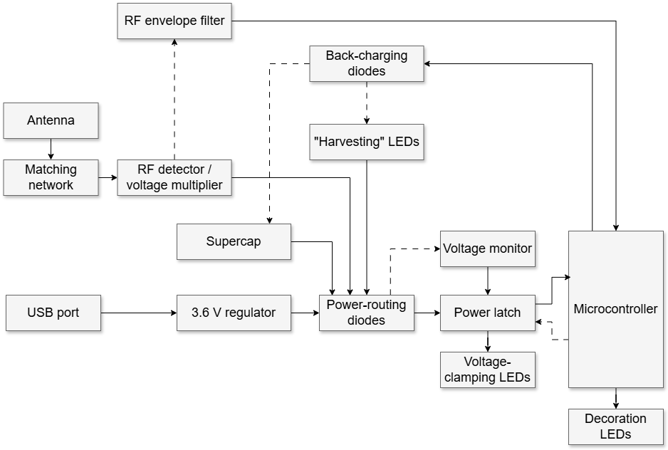
Block diagram of the card's hardware
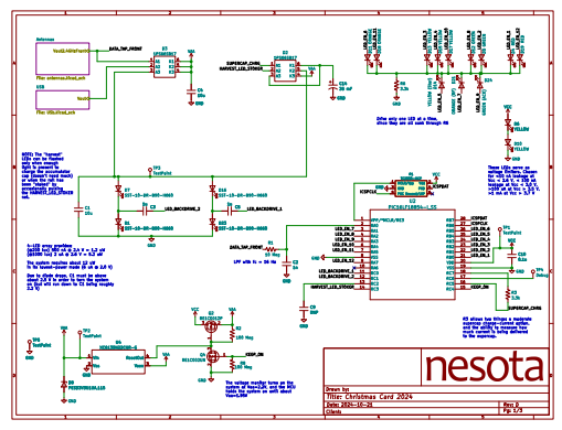
Schematic of the card
For harvesting power as well as receiving digital commands, the card includes what is essentially a simple 2.4 GHz radio made from a resonant circuit and some diodes. No local oscillators, no fancy filters, no active amplifiers; to a first approximation, it's like the classic "crystal radio" you might have built in childhood.
The radio really starts with the antenna, which is covered in depth later. For now, suffice it to say that the antenna is resonant at 2.45 GHz, so (handwaving here) it naturally is more efficient at receiving signals in that band.
The next step for the incoming signal is in an impedance-matching network, which makes the power transfer between the antenna and the rest of the receiver optimal, and does so preferentially centered at -- you guessed it -- 2.45 GHz. The matching network also has resonance of its own at 2.45 GHz, effectively (more handwaving) amplifying signals at 2.45 GHz and suppressing those far from 2.45 GHz.
At this point, there's a 2.45 GHz AC signal, but we need DC to power the card's circuitry. A single diode would be able to serve as a detector, rectifying some of the incoming signal into DC, but that single diode isn't very efficient. Instead, we'll use a two-stage voltage multiplier, a circuit topology that goes by many names and has been invented and reinvented seemingly a million times. The upshot is that we'll get about four times the peak-to-peak voltage of the signal coming out of the matching network, minus four diode drops. We're using good RF Schottky diodes (the Infineon BAT15-04W), so the forward drop per diode at the currents we care about is only about 150 mV at 10 uA (and under 100 mV at 1 uA). That minimizes losses in the diode and maximizes the voltage we can get out of the multiplier.
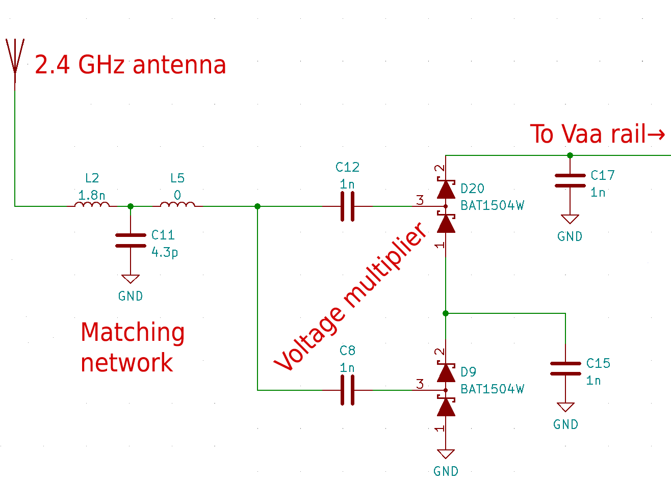
Annotated simplified schematic of the 2.4 GHz receiver frontend
We can simulate the voltage multiplier in LTspice using a model available on the Infineon BAT15-04W page linked above.
One subtle but important consideration when simulating the voltage multiplier is that the input to the anode of the first diode in the first stage must be allowed to swing around ground, so neither it nor the negative terminal of the simulated voltage source can be tied to ground directly.
At 2.45 GHz, with a 100 kohm load, the simulation reaches steady state in a few tens of microseconds:
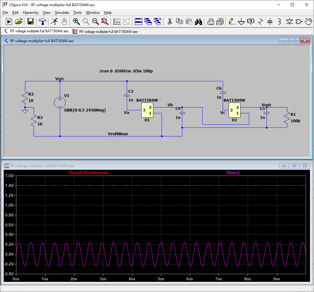
A 500 mVpp 2.45 GHz input signal (purple trace) produces a 1.4 V DC output from the voltage multiplier (pink trace) in a simulation of the circuit.
As expected, the output voltage is equal to four times the input peak-to-peak voltage minus four diode drops: (0.5 V * 4) - (0.15 V * 4) = 1.4 V.
Let's see how the simulation compares with reality. We'll probe a board that's had a u.FL connector populated on it and the antenna trace cut so that we can drive the input to the impedance matching network (and thus the voltage multiplier) with a signal generator. For easy comparison with the simulation, we'll use a 100 kohm resistor as the load instead of the normal complement of other board components. The signal generator's 2.45 GHz output was adjusted until 500 mVpp was observed at the input of the voltage multiplier.
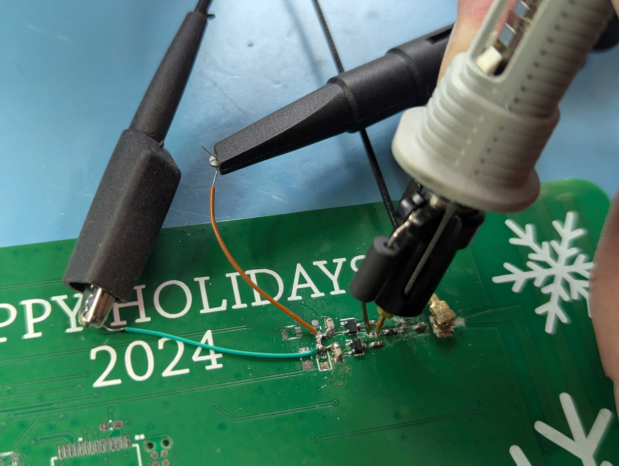
Probing the input to the voltage multiplier on the board. Note how a u.FL connector has been populated and the antenna trace partially scraped off so as to allow an external stimulus from a signal generator to be applied. Also note that a 100 kohm resistor is standing in for the system load.
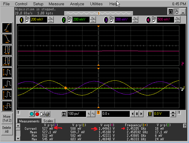
A 530 mVpp 2.45 GHz signal at the output of the impedance match, which is the input to the voltage multiplier (purple trace) results in 1.45 V DC out from the voltage multiplier (pink trace). This is in very good agreement with the simulation. (Ignore the yellow trace, which is being used only for triggering.)
The result: excellent agreement between reality and the simulation. The simulation produced 1.4 V from a 500 mVpp input, and in reality we got 1.45 V from a 530 mVpp input.
It turns out that putting 500 mVpp in at the antenna rather than at the input to the voltage multiplier actually results in about 2.6 V out from the voltage multiplier. The reason for that is the impedance matching network that sits between the antenna and the voltage multiplier, which, in addition to matching impedance, also resonates at 2.45 GHz. That effectively boosts the amplitude of the received signal, resulting in a larger DC voltage out.
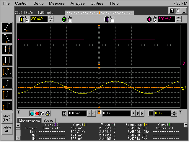
A 500 mVpp 2.45 GHz signal in at the u.FL connector (yellow trace) results in 2.6 V DC out from the voltage multiplier (pink trace)
A microwave oven works by converting electrical power from your wall into RF energy at about 2.45 GHz. Your food in the microwave oven absorbs that RF power, converting it to heat. The chassis and door of the microwave oven are very good at attenuating (blocking) that RF energy so that it can't get out and heat up undesired objects, but they're not perfect; some RF energy still leaks out.
Measuring exactly how much leaks out is tricky, but what we can say is that with a test card (having the u.FL connector populated) on the door, and the card's antenna connected to a spectrum analyzer via the u.FL connector, we found the peak received power to be about +5 dBm -- about 3 mW.
That leaked energy isn't enough to appreciably heat anything outside of the microwave, but it's plenty to light up the card's LEDs!
Powering the card using leaked 2.45 GHz signals from our microwave oven, about a foot away, while it was heating some water.
Even when you're not actively using the internet, your WiFi router sends messages out over the air about 10 times per second. With most routers having an effective radiated power of somewhere around +30 dBm, depending on some factors, those short idle bursts are plenty to power the Christmas card.
Here the card has been leaned up against the WiFi router's antennas. It's happily blinking away, being powered solely by WiFi traffic.
Want to see the card really light up? Do an internet speed test: the packets being sent by the router will be larger and more frequent, giving the card a lot more energy to harvest.
Of course, all of this depends on your phone or computer using the 2.4 GHz band of your WiFi network. Although your router almost certainly has the 2.4 GHz band enabled, it's possible (perhaps even likely) that your phone or computer is using a 5 GHz or 6 GHz band instead, as they generally provide higher speeds (albeit with other drawbacks). See the instructions page for more info.
The card is able to decode commands from the remote control web page when that page is accessed over a 2.4 GHz WiFi connection and the card is relatively close to the phone or computer accessing the page. It's able to do this without joining the WiFi network itself, and it's able to do it regardless of the encryption or access control in place on the WiFi network.
The way that control page is able to convey commands to the card is by modulating the amount of data being sent to a server set up for that purpose. When a lot of data is being sent rapidly, there's a lot of WiFi traffic, so the average power of the WiFi signal is high. When little or no data is being sent, there's not much WiFi traffic, so the average power of the WiFi signal is low.
In this way, basic amplitude-shift keying (ASK), specifically on-off keying, of the 2.4 GHz signal is possible. Extensive testing showed that each on or off period must be at least 150 ms to reliably distinguish between a "no carrier" state and a "carrier" state.
On the card side, the 2.4 GHz envelope is sampled at the output of the RF voltage multiplier stage and then passed through a 16 Hz first-order low-pass filter. This cuts down the noise somewhat while also obviously limiting the modulation rate (but to be clear, the modulation rate was set first, then the values for the LPF were set later).
The prototype implementation of the remote control web page sent data in 5 KB chunks using POST requests. However, there was a lot of overhead with that approach, and timing jitter was terrible, so we eventually changed the implementation to use a websocket connection that is left open, and data is either streamed or not streamed to the websocket. The websocket acts simply as a black hole; all data received is immediately discarded. Latency is much, much better with the websocket approach versus the POST approach.
As you can see on the remote control web page, the user is given several options. The most basic, "power on", starts streaming data to the websocket, allowing the card to be powered from the phone assuming it is positioned appropriately. If the user then chooses one of the command options (e.g., "enable tree star"), a script on the page assembles a frame corresponding with the chosen command and modulates the data being sent to the websocket according to whether a 1 or a 0 needs to be sent in a particular bit time. If a 1 needs to be sent, data is streamed to the websocket. If a 0 needs to be sent, no data is streamed to the websocket, but the connection is left open.
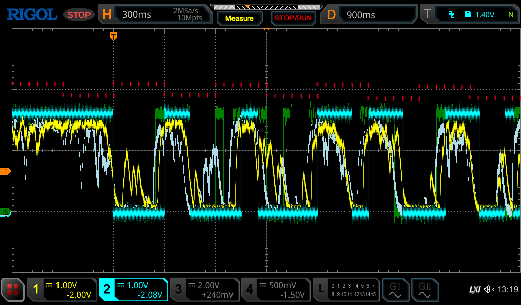
Scopeshot showing two instances of the low-pass-filtered 2.4 GHz RF envelope during a command from a phone (yellow and gray -- same command both times), the output of the comparator for those two envelopes (blue for yellow, green for gray), and the annotations of the sampling times (red, every 50 ms).
A data frame consists of 8 synchronization bits in a Barker-7 sequence (plus a leading 1), followed by 16 bits that encode the codeword. There are 8 valid codewords, resulting in 3 net data bits. Barker codes have very low autocorrelation sidelobes, meaning that their autocorrelation is very low unless the alignment is perfect. This makes them very good for synchronization, which is how we're using the Barker-7 code here.
The codewords were developed by exhaustively searching for 16-bit values with specific characteristics: no runs of more than three 1s, no runs of more than two 0s, a Hamming distance of at least 6 between any two codewords as well as between any codeword and the all-zeros or all-ones cases, and at least a moderately high Hamming distance between any code shifted by +1 or -1 bits and any other code.
The eight codewords in binary, sent most-significant bit first, are:
On the card, the RF level is monitored at a pseudorandom interval, usually several times per second, and the comparator slicer level is set to half of the peak value seen over the past eight observations.
No RF decoding is attempted unless the observed RF level is above a threshold corresponding to about 300 mVpeak at the RF level ADC input, though since the RF level is relative to Vcc, this can vary. The RF level measured for the slicer is also used to set how rapidly the orange RF Level LED flashes (and if at all).
If the RF level is above the threshold, then on every system tick (i.e., every 50 ms) the RF input is sampled with the comparator and the new bit is shifted into a circular buffer. The buffer is then checked for correlation with the Barker-7 sequence. By sampling the 150 ms period modulation from the phone at a rate of 50 ms, the card is able to recover the clock sufficiently well while doing so in a very power-efficient manner.
If a sufficient correlation with the Barker-7 sequence is found, an attempt to decode the payload of the frame is made. The payload is checked for correlation against all eight valid codewords. The codeword with the highest correlation, and which also exceeds a minimum cutoff correlation, is selected as the most likely codeword, and the command corresponding to that codeword is executed.
The green LED near the "2024" text on the front of the card is flashed when a valid command has been received and processed. For commands that affect the card configuration, the relevant non-volatile settings are updated in the PIC's EEPROM.
Valid numerical commands are:
Commands 0 through 5 are idempotent, which means that they can be sent multiple times with no adverse effects.
There are a variety of challenges with the approach of modulating a WiFi signal's magnitude using streaming data. Network congestion, browser stalls, and retries all contribute to timing jitter. Extra traffic, even routine traffic, from the phone leads to extra 1s effectively being sent. The distance between the phone and the card, or the relative orientations of the two devices, can change, leading to drastic changes in signal strength, resulting in improper slicer levels and missed bits.
However, the biggest challenge isn't technical per se: it's that use of 2.4 GHz WiFi networks has fallen out of favor, and it can be a challenge to force a phone to use a 2.4 GHz network when the SSID is shared with a 5 GHz network.
Many modulation, encoding, error-correcting, and error-detecting techniques were investigated before landing on what's now in the card. Timing jitter, fading, noise (especially burst noise), decoding complexity, and the slow minimum modulation period all ended up being showstoppers.
Some phones, most notably several made by Samsung, appear to incorporate a sort of time interleaving to share the 2.4 GHz band between Bluetooth and WiFi. On those phones, continuous WiFi data transmissions are interrupted about twice a second for about 100 ms at a time. This wreaks havoc with the modulation scheme used on the card. Fortunately, there's a simple work-around: temporarily disable Bluetooth.
Usable range for the remote-command feature depends on whether the card is being powered via RF from the phone versus being powered from USB or the supercap. If the card is being powered by the RF from the phone, range is pretty short; the card must be touching the phone. If the card has a separate source of power, like USB or the supercap, range can be several feet.
The original plan was to include five antennas: three for 2.4 GHz (one on the front and two on the back) and two for 5 GHz. They were all going to be "patch" antennas, as that design has high gain.
FDTD simulation of the front 2.4 GHz patch antenna on an earlier prototype of the card in response to an impulse stimulus. This clearly shows the oscillation of the magnitude of the E-field on the board (red is stronger) as well as isolines ("blobs") of the E-field propagating away from the antenna. This animation covers a few nanoseconds of time.
However, issues with manufacturing tolerances, high losses at 5 GHz, and -- most importantly -- a need to drastically reduce a ballooning part count led to an eventual reduction to a single antenna. That "meander" antenna, now located on the right side of the card, was based on one in a Texas Instruments app note (DN024), with further modifications after simulations in the OpenEMS electromagnetic field solver due to the change in orientation and board size relative to the reference design.
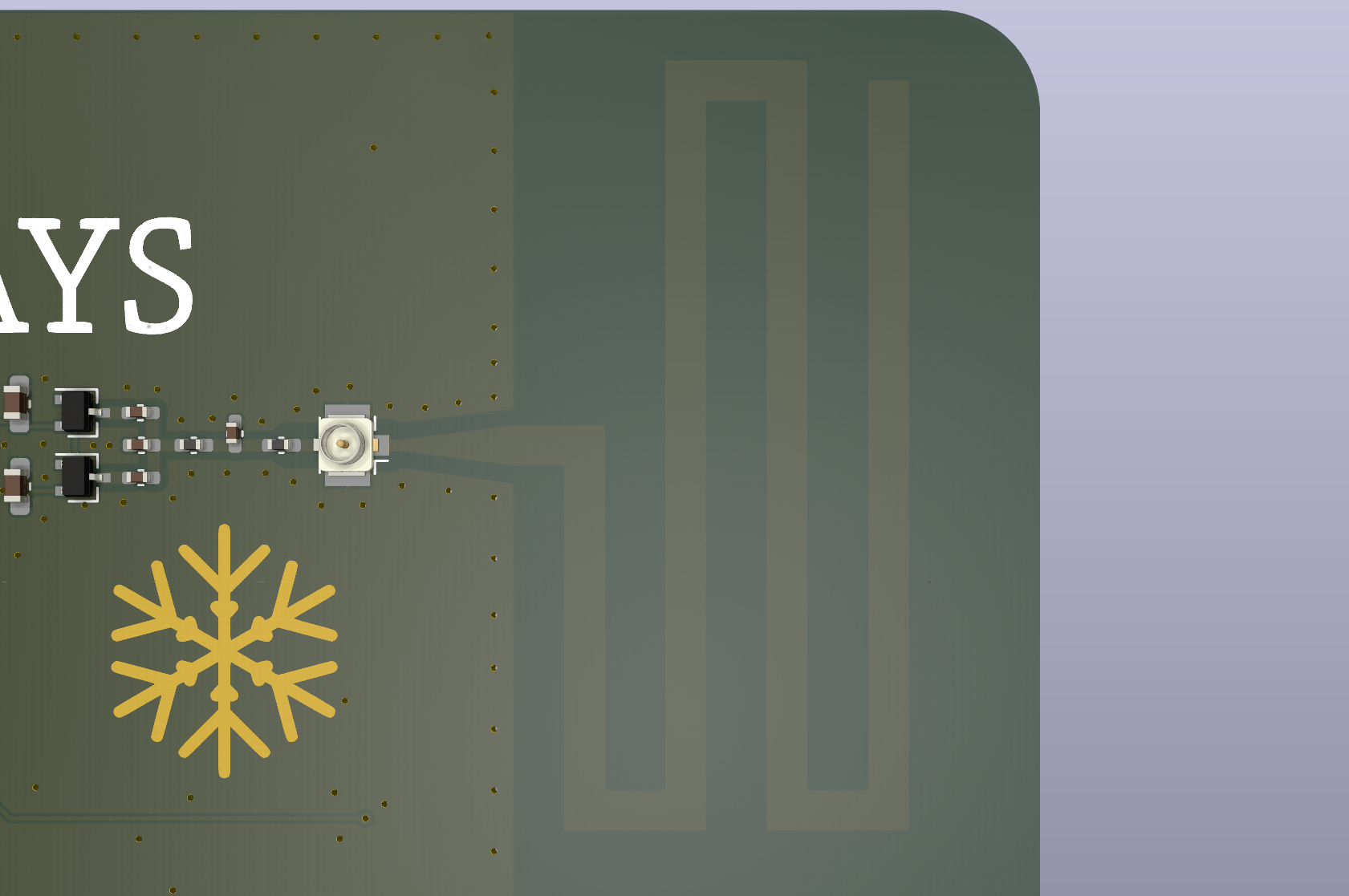
The 2.4 GHz meander antenna
FDTD simulation of the card's antenna, as viewed from the front of the card. The colors are increasingly red with increasing E-field magnitude. Note how you can see the antenna oscillate. Also note how the ground plane shows a non-zero amount of interaction with the signal: it occasionally grows slightly lighter, revealing its copper outline on the fiberglass PCB substrate. This animation covers a few nanoseconds of time.
The final antenna has its main lobe to the right of the card, with vertical polarization. Maximum gain in the main lobe based on the simulation is about +3.8 dBi.
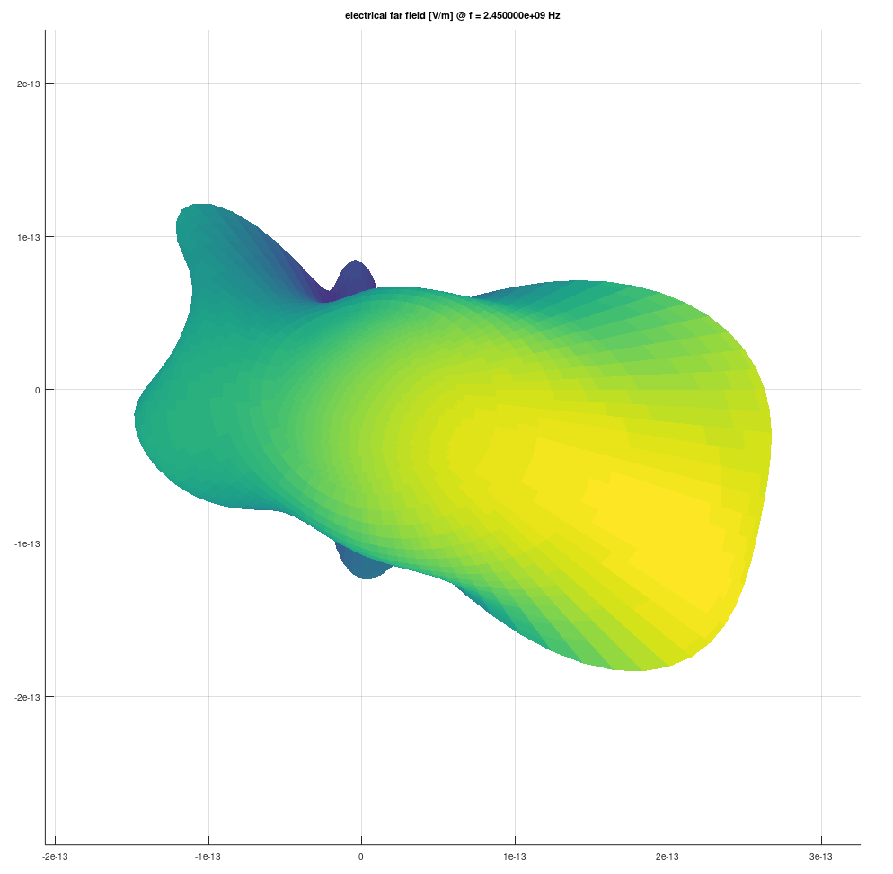
Simulated antenna radiation pattern at 2.45 GHz (viewed looking down at the front of the card along the Z-axis)
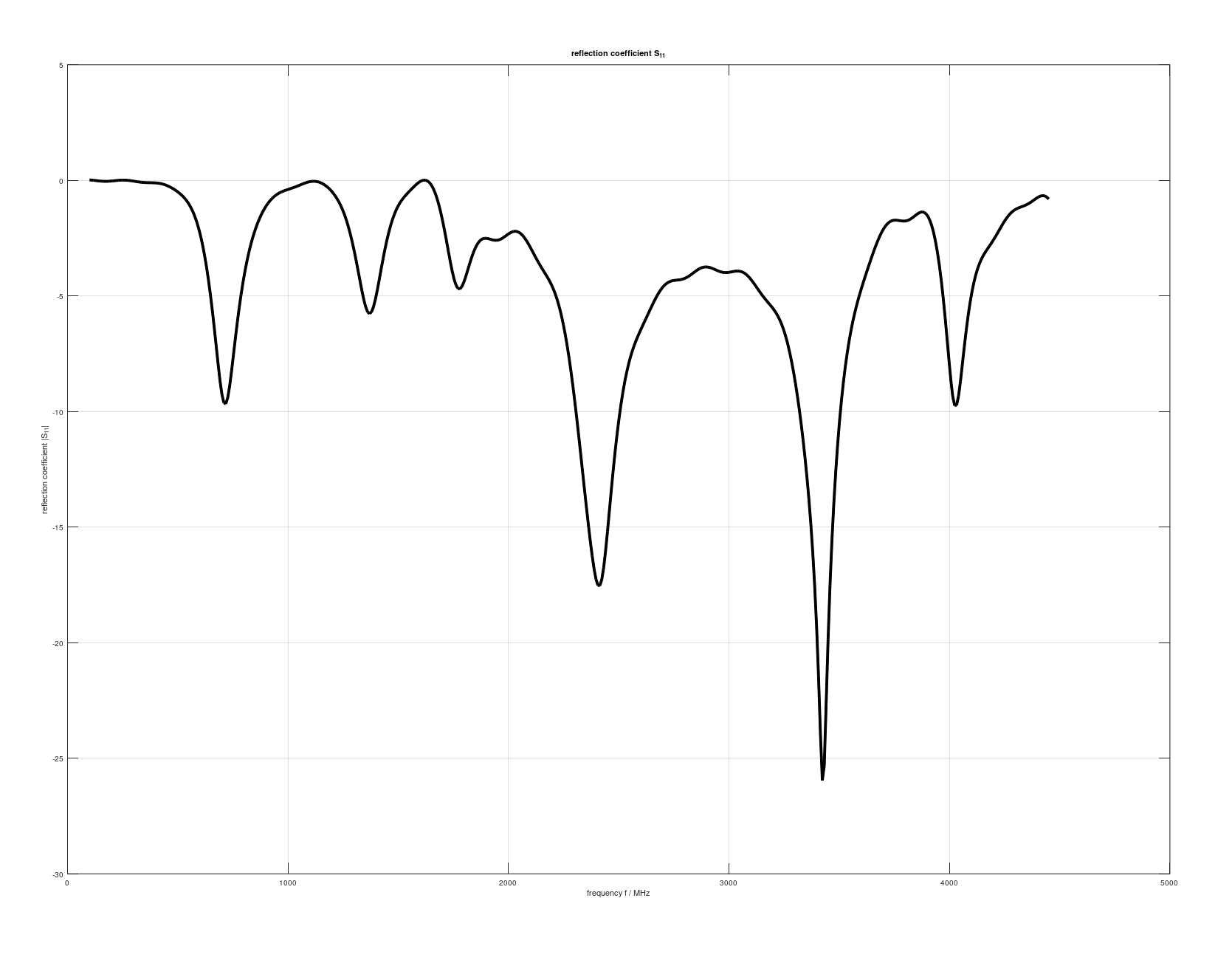
Simulated antenna S11 return loss (note that this chart goes to 5 GHz, unlike the VNA screenshot below, and is 5 dB/div instead of 10 dB/div)
The antenna on the final board matched the simulation very well, as measured directly with a vector network analyzer (VNA).
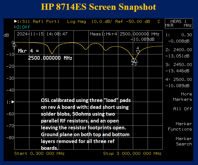
S11 return loss of the antenna (actual); lower is better. Decent match throughout the 2.4 GHz band (S11 RL values lower than -10 dB are generally considered "good" in the context of antenna matching)
Matching the antenna to the RF detector was accomplished using a T-network, though extra footprints were included in case a more complex matching network ended up being needed. A VNA was used to evaluate the state of the match and provide directional guidance, but ultimately iterative optimization by placing, soldering, measuring, desoldering, and replacing matching components was required. The final match was very decent for the 2.4 GHz band.
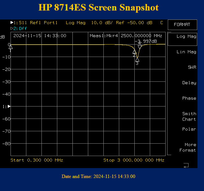
S11 return loss of the matched RF detector (actual). Markers 1, 2, and 3 are at 2400, 2450, and 2500 MHz, respectively. Note the resonance (local minimum) at 2450 MHz.
About two dozen different models of LEDs were screened on the bench to see which ones were best suited for acting as little solar cells. The parts eventually chosen for the "harvest LEDs" were almost four times better than the next best option in terms of output power for a given incident light level.
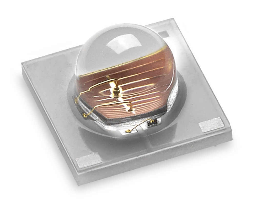
One of the light-harvesting LEDs. Note the large lens and large die. (Photo: Luminus, Inc.)
Open-circuit, each one of those four big red LEDs will produce about 1.4 V in almost any light, and each one will move about 200 nA of current in 200 lux. Since current is proportional to illuminance, that increases to several microamps at around 1000 lux and can reach many tens of microamps in even brighter conditions.
A video Jeff made going into more detail about how LEDs can be used as little solar cells
In order to produce sufficient current at sufficient voltage without needing any sort of DC/DC converter, the four harvest LEDs are arranged in two parallel strings of two series LEDs.
The really neat trick is that the system can be powered off of the harvest LEDs and also blink those same LEDs using energy harvested from them.
Blinking the harvest LEDs is accomplished by sending one full cycle of an AC-coupled signal back into the harvest-LED network. The "high" side of the cycle turns on the "low" harvest LEDs, and the "low" side of the cycle turns on the "high" harvest LEDs.
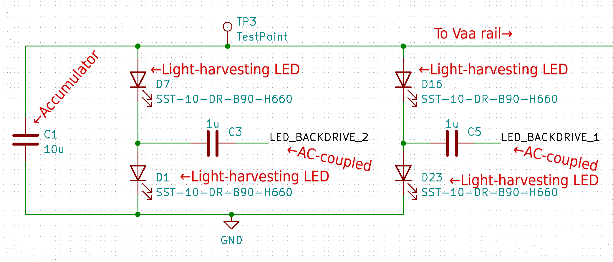
The arrangement of the light-harvesting LEDs on the board.
One additional complication is that to blink the harvest LEDs the 10 uF light harvest accumulator capacitor must be charged to at least 1 V or so. When the card is in a normally lit room, the harvest LEDs themselves produce enough voltage to charge that cap to a sufficient potential, but when the card is in a pitch-dark room, running off of another power source (e.g., RF or USB), that cap has little to no voltage across it. To address this, the microcontroller is connected to that rail via a diode, and the firmware will occasionally send a short pulse of energy to the harvest accumulator capacitor, thus ensuring that it's at a high enough potential to enable the harvest LEDs to be lit using the AC-coupled signal.
The card is shown here running purely on light, about 1000 lux. It will run with less light; the interval between bursts of blinking will simply get longer as light levels go down. Although the big light-harvesting LEDs have the most noticeable blinks, several of the smaller LEDs can also be seen blinking occasionally. They can be hard to see if you're not watching for them; can you find all of the blinks?
There is a supercapacitor (supercap) on the card, allowing the system to run without any other sources of energy when charged up. The supercap can be charged more rapidly than a lithium battery of the same form factor, and it can be recharged an almost indefinite number of times. It is not needed for the normal operation of the card and serves simply as an optional use mode.
The supercap is a Seiko XH311HU, which has a value of 35 mF and a maximum voltage of 3.3 V. As used on the card, it can be charged to about 3.0 V under normal conditions (e.g., when the card is plugged in to USB) and as high as 3.3 V under exceptional conditions (e.g., when in the presence of strong RF for an extended period of time).

The XH311HU 35 mF supercapacitor (Photo: Seiko Instruments)
The typical charge rate is about 30-100 uA, though it can go as high as 1 mA when starting from dead-flat. In order to prevent excess load on the system while operating in a limited-power situation, the system doesn't charge the supercap unless the supply rail is 2.7 V or higher, which is the case only while powered via USB or in the presence of a consistently strong RF field.
When charged to 3.0 V, it will provide as much as 2.75 V to the Vaa rail, and with the minimum run voltage of the system being about 1.95 V, that gives a useful swing of about 0.8 V. Under those conditions, the supercap can power the board on its own for about half an hour.
A decent amount of logic is employed in the firmware to protect the supercap from charging above 3.3 V, though that's very much a corner case.
The name of the game with this project was "power management". Everything about the design, from the hardware component choices to the specific way the firmware was written, was done with an eye towards efficiency.
A major design consideration was how to avoid backpowering the microcontroller. Stated differently, the design needed to avoid powering the microcontroller through its IO ports, which happens because of the internal protection diodes that are on all of the microcontroller's IO pins. When the microcontroller's main power supply is absent, it's still possible to power it by having a high enough voltage on one or more of the microcontroller's non-power pins. That's undesirable when we're trying to keep the microcontroller powered off.
The problem was especially important and apparent when trying to charge the system off of light, since even tens of nanoamps in that state are significant. Parasitic loads from backpowering the microcontroller or anything else would easily prevent the system from running on light. The solution needed to be not only effective but also cheap, as a higher part count would lead to both higher direct costs as well as added assembly time. Although power control based on MOSFETs was considered, ultimately a network of Schottky diodes was chosen.
The drawback to Schottky diodes is that, for the ones used on the card for power control (instead of RF detection) and at the currents relevant to this project, they have forward drops of between 100 mV and 350 mV, We're already struggling to get and keep the voltage high enough without any sort of boost converters, so that's a signiciant drop of voltage. The benefit of a diode-based solution is simplicity: a diode needs just a diode, whereas a FET-based solution needs two FETs and two resistors. In addition, depending on how the FETs are controlled, more power might be lost in the gate pull-down/up resistors that would be lost to the voltage drops across the diodes.
Transient overvoltage protection from electrostatic discharge (ESD) events takes the form of a 3.3 V TVS diode on the Vaa rail, which as described elsewhere is usually shorted to the Vcc rail.
However, several of the components, notably the microcontroller, have absolute maximum ratings of 4.0 V, and the TVS diode won't actually start conducting until about 5 V or so. To keep the rail voltage from getting higher than about 3.7 V, and to provide extra visual interest, a technique that Jeff first saw used in a solar-powered calculator was employed: using two forward-biased LEDs in series to clamp the voltage while keeping leakage extremely low. That's the purpose of the two yellow LEDs in the middles of two of the snowflakes.
When the voltage is below about 2.6 V, their actual measured leakage current is inconsequential (less than 10 nA), and the leakage is still below 100 nA as high as 3.0 V. However, when the voltage gets above about 3.5 V, their forward current becomes significant, and they effectively clamp the voltage to about 3.7 V even when the card is in the presence of very strong RF.
When the amount of available power is insufficient to run the card continuously, such as when no power source other than relatively dim interior lighting is available, the system accumulates charge while keeping parasitic drains to an absolute minimum. Once enough charge has been accumulated to raise Vaa (the main supply rail) to 2.2 V, a Torex XC6135 ultra-low-power voltage monitor connects Vaa to Vcc (the main load rail) by pulling the gate of a P-channel FET low, powering the microcontroller and causing the firmware to boot.
Within about 10 ms of Vcc rising above the brown-out reset (BOR) threshold of the microcontroller, the firmware will latch the Vaa-to-Vcc connection pCh FET by pulling the KEEP_ON line high, which causes an N-channel FET to pull the pCh FET's gate low in parallel with the voltage monitor's output. That will keep the system powered on so long as the firmware wants it to be so, regardless of what the voltage monitor does from then on.
In order to monitor the Vcc rail voltage to ensure that it's still high enough to safely run, but to avoid paying the 9 uA penalty for enabling the microcontroller's brownout (undervoltage) detection hardware continuously, the firmware enables the brownout detection hardware for about 1 ms every 50 ms -- long enough to successfully turn off if the voltage goes too low, but without the power penalty. If/when the brownout detection puts the microcontroller into reset, the KEEP_ON line will immediately float, disconnecting Vcc and Vaa. At that point, with no load on Vaa, Vaa is able to slowly accumulate charge until there is once again enough charge to start the whole process over.
Under about 500 lux of light, it takes about 7 seconds to accumulate enough charge to turn on the microcontroller. Once running, the accumulator caps will provide enough energy to continue running for between about 500 ms and 1500 ms, depending on which LEDs end up getting randomly blinked (some have higher drains than others).
The total drain of the system while "off" (with the microcontroller in reset and Vcc disconnected from Vaa) is about 100 nA, as measured with a SourceMeter, almost entirely due to the quiescent current of the voltage monitor.
When on with Vaa driven to 2.3V with a SourceMeter, but with the LEDs disabled for testing, the voltage monitor draws about 200 nA, the pull-up/down resistors on the power-control FETs draw about 20 nA each, and the microcontroller draws about 4 uA. Reverse leakage through the power-control diodes is about 10 nA per reverse-biased diode.
There are two configurable power modes for the output LEDs. "Normal" mode blinks a random LED on the tree for a random amount of time between 0.25 and 1.75 ms, and does that 10 times per second. "Ultra-high-power" mode does something similar, except the maximum blink time is 7.75 ms and the blinks happen 20 times per second.
Regardless of the configured power mode, blink durations are restricted to no more than 1.75 ms when the supply rail is below 2400 mV or the system has been up for less than 2 seconds.
Astute observers might note that the LEDs are configured in a common-cathode arrangement. This was done in order to be able to use the "weak pull-up" GPIO drive mode of this microcontroller to dimly light one or more LEDs steadily and concurrently, as the discrete 3.3k limiting resistor is basically a short to ground compared to the weak pull-ups. However, that mode ended up not being used.
The firmware was written in C using a "bare metal" approach for a PIC16LF18854 microcontroller. The compiled code uses about 3452 words of program flash and about 150 bytes of RAM, plus 3 bytes of EEPROM. This specific microcontroller was chosen for its combination of low cost, very good power efficiency, and a rich suite of onboard peripherals. It also helped that Jeff was already quite familiar with PIC16s and their quirks.
If you'd like, you can peruse the source code for the firmware. Beware that's it a quick hack, so it's rather ugly. Also, there are many atypical practices in that code that boil down to two things: first, techniques applied for the sake of power efficiency; and second, techniques to work around the terrible optimization applied by the XC8 toolchain.
When the system boots up, the first thing the firmware does is pull the KEEP_ON line high, thus ensuring that the microcontroller will continue to receive power even if the voltage drops low enough for the separate voltage monitor chip to turn off. The microcontroller can run down to about 1.95 V before BOR, 1.8 V per the datasheet, and about 1.7 V if you really push it, but the voltage monitor is configured to turn off (and on) around 2.2 V with very little internal hysteresis -- hence the need for the "keep on" feature. More details here.
The clock speed is normally 15.5 kHz -- yes, kilohertz -- but is temporarily increased to 16 MHz while servicing a system tick, which happens 20 times per second. The microcontroller core itself is stopped between interrupts, but the system clock continues to run for the sake of several peripherals.
The choices of 15.5 kHz and 16 MHz were arrived at by directly testing various options, including 32 MHz on the high side and all the way down to 968 Hz on the slow side. There were diminishing returns in terms of power savings going below 15.5 kHz. On the fast side, going from 16 MHz to 32 MHz made execution take half as long, as expected, but the peak current doubled, so we limited the clock to 16 MHz to reduce supply-rail droop.
The main disadvantage of the 15.5 kHz mode, other than executing about 4000 instructions per second (roughly the speed of ENIAC, the first electronic general-purpose computer), is interrupt latency. It takes about 7 ms to start servicing an interrupt when coming out of idle mode at 15.5 kHz. Since the LEDs need to be blinked for about an order of magnitude shorter than that, a third system clock frequency is used while waiting for a blink timer to expire: 1 MHz. After the blink is over, the system goes back to 15.5 kHz until the next system tick wakes it up again.
The code itself takes great pains to limit the number of instructions executed every system tick. For most critical sections, several approaches were tried and the resulting assembly code analyzed to determine which option would take the least power. Everything is integer math, and, as much as possible, multiplications and divisions are limited to powers of two (which can be done with rotates). To illustrate why that's important, dividing a 16-bit number by an 8-bit non-power-of-two number consumes about 500 nJ (nanojoules) of energy, about the same amount of energy as to blink one of the LEDs(!). However, dividing that same 16-bit number by a power of two takes about an order of magnitude less energy on this microcontroller, about 50 nJ (depending on the details).
Random numbers come from a simple pseudorandom number generator based on a LFSR, seeded at startup and every 12 seconds or so using the noisiest bits of the ADC sampling the supply rail. The main use of those random numbers is in selecting which LED will be blinked on a tick.
There were three rounds of prototypes before the final board spin
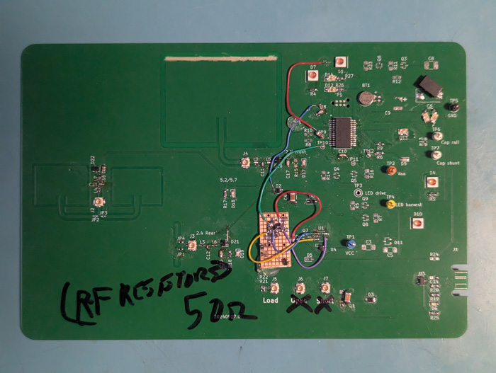
First prototype board
The first prototype, circa September 17, 2024. This was mostly a platform for experimentation. Note the protoboard that's stuck on top, which added the FETs to allow the microcontroller to hold power on even after the voltage dropped below the discrete voltage monitor's threshold. Several patch antennas are visible, including two meant for the 5 GHz WiFi band. At this point, a small rechargeable battery was still on the board, visible in the upper right ("BT1").

Second prototype board
The second prototype spin did away with the 5 GHz antennas and the front 2.4 GHz patch antenna, adding a meander antenna instead. There are still two 2.4 GHz patch antennas on the back. The supercap made an appearance, but an oversight meant that it wouldn't let the microcontroller properly reset when the voltage drooped below the brown-out voltage. Several flywires are visible for probing test points. The sketch of the tree and us was meant to be a placeholder, but we kind of liked it, so it stuck around with only minor revisions.

Third prototype board
The third prototype spin settled on just a single antenna, now on the right side of the board so that it has vertical polarization. Silkscreen over the antenna caused both tuning and damping issues; in this photo, it has been scraped off. The USB-C contacts are inverted, so it works only with a USB-C-to-A cable (which is why we didn't notice earlier). A few LEDs still aren't in their final positions. The board is otherwise very close to its production state.

Fourth iteration: the board as released
The fourth iteration became the board you all received. It fixed the antenna tuning/damping issues, moved a few LEDs around, added some more snowflakes, and fixed the USB connector issue. Three component footprints remain unused: one for an unneeded bulk capacitor, one for a u.FL connector for tuning, and one for an unneeded impedance-match capacitor.
Sean and Jeff assembled all of the boards by hand here in Denver, almost entirely under a stereo microscope. The "manufacturing" time per board, including prep, soldering, flashing the firmware, several rounds of testing, cleaning, and packaging for shipment, was about 45 minutes. We built 99 boards; one PCB was sacrificed to the RF-tuning gods. Total time spent on the project, including engineering and assembly, was somewhere around 300 hours.
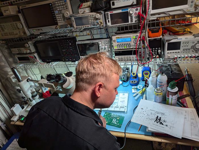
We assembled all of the boards by hand
The bare PCBs were manufactured by PCBWay in Shenzhen. They are two-layer 0.8 mm boards made of FR4 finished with the electroless nickel immersion gold (ENIG) process, basically gold plating, primarily for aesthetics.
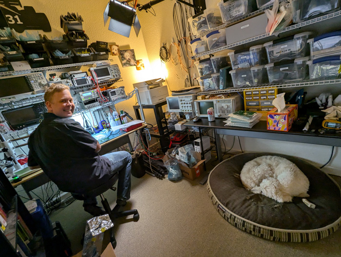
Sophie supervised the assembly
Why not use a vendor to assemble the boards? Cost and timeline. You can have it done cheap, but you'll be waiting a while, or you can have it done fast, but it will be very expensive. As we were unable to pull in the timeline and unwilling to pay the extra cost, we assembled them ourselves.

Packaging the cards for shipment. Also: Sophie!
Perhaps amusingly, and perhaps as a direct result of the abuse we put ourselves through hand-assembling the cards, we got this little gem (a pick-and-place machine, plus a reflow oven off-camera!) the day before we sent the cards out. Too late to make a difference this round, but oh, the possibilities for the future!
After assembly, each one of the boards was subjected to a basic smoke test by applying 5 V current-limited to 5 mA across the Vbus and ground pins on the USB connector. If the board showed current consumption of 500 uA +/- 50 uA, it moved on to programming, in which the firmware image is flashed to the microcontroller. After programming, each board was connected to a USB power source; the firmware on the board would then detect it was in a first-boot condition, and it would jump into a self-test mode.
In the self-test mode, all of the tree LEDs were lit automatically in sequence, very brightly, so that they could be visually verified for functionality. Meanwhile, the voltage rails were checked to be within expected limits. If the rails looked OK, charging of the supercapacitor was enabled and the current going into the supercap was checked to be within expected limits: too high, and that would indicate a likely short. Too low, and that would indicate an open. If the supercap charging looked good, the board would move on to check for RF signals, in which it would look for an RF level that would be consistent with having a cell phone in the "remote control power on" mode roughly 6" away from the right side of the card.
During the self-test, the orange RF activity LED to the right of the text "2024" blinks the number of the step the test is on. When the final step of the test has been completed, a flag in EEPROM is set so that the board won't start in self-test mode on the next boot, and the green LED to the right of the text "2024" blinks rapidly.
It is possible to enter self-test mode by sending a pair of "advanced" values from the card control page: send "7", then wait for the green acknowledgement, then send "6". Be sure the card is plugged into a USB power source when the self-test mode is active, or else it will effectively continuously reboot after lighting the top few of the tree LEDs.
As a fail-safe, self-test mode is automatically disabled for the next boot if the system runs for 30 seconds continuously.
Overall, first-pass yield was about 90%, and two-pass yield was 100%. There was one instance of two pins being shorted together, one damaged LED, one LED installed backwards, several cases where components were only half soldered down, one case of damage during cleaning, and one extremely puzzling case of a short in the PCB itself.
That last one consumed an hour of diagnostic time and involved using time-domain reflectometry (with a 20 ps rise-time pulser and 20/50 GHz scope) to locate the fault to within a region of a couple millimeters on one trace. Nothing ever became apparent visually, even under high magnification, but the problem spontaneously resolved after the soldermask had been scraped away in that area. As best we can figure, some extremely small conductive contaminant had found its way into the soldermask.